
Research Signal – Source date 2024-05-23
A radiation detector can absorb an incoming gamma ray yet lose some of the light that would reveal its arrival. Inside a scintillator—a material that turns ionizing radiation into light—photons can bounce repeatedly off the crystal’s boundaries. Some are reabsorbed before reaching the light sensor. Producing light and delivering a useful electrical signal are separate steps.
That distinction anchors a review published on May 23, 2024, Bright Innovations: Review of Next-Generation Advances in Scintillator Engineering. It brings together approaches that change a scintillator’s surface or internal structure, extending the familiar strategy of changing its chemical composition. The contribution is a comparison of physical mechanisms, supported by a mixture of experiments, calculations, and early material demonstrations.
“Brighter” and “faster” can therefore describe different achievements. A surface pattern may let more existing light escape. An engineered optical environment may change how quickly light is emitted. Alternating materials may add an early pulse that helps establish when radiation arrived. Those improvements occur at different points between absorption and detection, and require different measurements to establish them.
Giving trapped light a way out
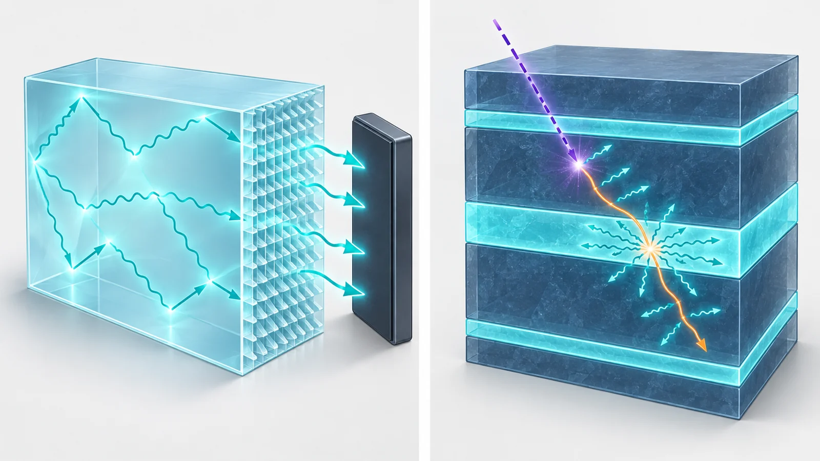
Many scintillators use dense materials containing heavy elements because they absorb high-energy photons effectively. These materials also commonly have a high refractive index, which describes how light propagates through them. At an interface with air, the large index difference means light approaching the surface at sufficiently oblique angles is reflected back inside. This is total internal reflection.
Optical grease between a crystal and its sensor can reduce that mismatch. But the interface remains an important design problem, particularly when a camera must collect light remotely from a scintillating screen rather than through direct optical contact.
Photonic crystals offer another route. These are repeating structures with spacing roughly comparable to visible-light wavelengths. Applied to a scintillator’s surface, patterns of holes, pillars, or tiny spheres can redirect light that would otherwise remain trapped. Their geometry changes the directions in which light can leave the material.
The review summarizes experiments in which a scintillator known as LYSO received patterned titanium dioxide coatings. Different hole patterns produced reported light-output increases of 53% and up to 70%. These are gains in the measured light signal under the respective study conditions. They do not, by themselves, mean the material generated that many more photons internally.
Pattern dimensions matter because light interacts with the whole structure. Hole size, spacing, height, and the coating’s optical properties all affect extraction. The optical connection to the sensor matters too. A reported percentage therefore belongs to a particular patterned sample and reference arrangement; it is not a general multiplier that can be assigned to every detector using that coating.
Changing emission before the light travels
Surface extraction addresses photons after they have been produced. The Purcell effect reaches an earlier part of the process: the surrounding optical environment can alter spontaneous light emission itself.
In a carefully designed layered structure, alternating scintillator and spacer materials change the optical states available for emission. Adjusting their thicknesses and refractive indices can favor emission in useful directions and increase its rate. This is a different physical job from redirecting trapped photons at an exit surface.
One theoretical study summarized in the review calculated a fivefold increase in detectable photons for a layered LYSO structure compared with bulk LYSO, together with faster emission. It also calculated a 2.4-fold improvement in coincidence timing resolution, a measure of the precision with which a detector pair measures the relative arrival times of two radiation events. These are predictions for the modeled architecture, rather than measured gains from a fabricated detector.
The calculation also exposes a demanding construction requirement. In an 800-layer structure about 220 micrometers thick, layer-thickness variation with a standard deviation of just 6–7 nanometers destroyed the modeled effect. A promising optical design can depend on dimensions that are difficult to reproduce across hundreds of layers. Even successful control of emission would leave the sensor and readout electronics contributing to the final timing measurement.
Adding an early pulse through neighboring layers
A second layered approach divides the work between two materials. A dense scintillator absorbs radiation efficiently, while an adjacent fast emitter supplies prompt light. The connection between them is the motion of energetic electrons generated after radiation absorption.
If the layers are thin enough, an electron can travel across their boundary and deposit energy in both materials. The fast component then adds early photons to the main scintillation pulse. Researchers call this energy sharing. Its effectiveness depends on whether individual radiation interactions actually distribute energy across the layers.
An experiment summarized by the review combined 100-micrometer plates of the dense scintillator BGO with 200-micrometer plates of EJ232 plastic. A detector pixel measuring 3 × 3 × 15 millimeters achieved a coincidence timing resolution of 197 picoseconds, compared with 271 picoseconds for the bulk-BGO reference. A picosecond is one trillionth of a second; a smaller timing-resolution value indicates a narrower spread in the measured time difference.
That comparison gives the mechanism a concrete experimental anchor. Unlike the calculated photonic-layer enhancements, it is a reported detector timing result. It still belongs to its particular experiment: pixel dimensions, light collection, sensors, and data processing can affect timing values, making reference samples essential when comparing studies.
The plastic brings a physical cost. It is less effective at stopping gamma rays than the dense crystal it partly replaces. The review also identifies a low fraction of energy-sharing events as a limitation. A detector must absorb enough radiation and produce useful timing information across its events; selecting a fast emitter alone does not settle that balance.
Why a fast nanocrystal flash is only part of the answer
Nanocrystals are candidates for the fast-emitting component because confining electronic excitations within tiny crystals can favor rapid light emission. The review discusses hybrids involving materials such as cadmium selenide and lead halide perovskites alongside conventional bulk scintillators.
Here, the way a sample is excited matters. Photoluminescence is light emitted after optical excitation. Radioluminescence is light emitted under ionizing radiation. An optical experiment can reveal useful emission behavior, but a radiation detector must also absorb the incoming radiation, transfer its energy, and deliver a measurable pulse.
The review describes a preliminary hybrid made by depositing cesium lead bromide nanocrystals onto a conventional scintillator wafer. A light-emission component with a decay time below one nanosecond appeared under both optical and radiation excitation. That observation supports the presence of a fast component under relevant excitation; it does not measure the timing precision of a complete detector pair.
The proposed destination of 10-picosecond coincidence timing must be read separately from those early results. Emission decay time describes how a light pulse fades. Coincidence timing resolution describes the spread in measured event-time differences. Establishing one does not establish the other, even when both are expressed in very small units of time.
Fine patterns must survive a thick detector
The fabrication challenge spans very different scales. Photonic structures need features comparable to light’s wavelength. Energy-sharing layers must permit electrons to cross between materials. Meanwhile, the complete detector needs enough absorbing material to intercept the radiation of interest.
For 511-kiloelectronvolt gamma rays used in positron emission tomography, or PET, the review discusses scintillator thicknesses of at least 10–20 millimeters. That is a very different construction task from demonstrating an optical effect in a thin film. Building up sufficient thickness must preserve the internal geometry and avoid excessive production time.
Thickness also creates an optical problem for some candidate materials. The lead halide perovskite layers discussed in the review are generally below about 100 micrometers. Making them thicker would increase absorption of incoming radiation, but their own emitted light can be reabsorbed before escaping. More absorbing material can therefore make light transport harder. Patterning and changes to the nanocrystals are among the approaches considered for managing this tension.
Manufacturing methods solve different parts of the problem. Nanoimprinting can reproduce fine patterns at potentially high throughput, but requires materials suitable for imprinting, such as polymers or nanocrystal inks. Focused ion beams can pattern many materials precisely, yet their speed and expense constrain large-area production. Self-assembly offers a route to extensive thin patterns, while maintaining order throughout a large three-dimensional crystal remains difficult.
Printing introduces another distinction. Demonstrated scintillator printing with features on the order of hundreds of micrometers may suit some energy-sharing architectures, but those features are too large for the photonic effects under discussion. Higher-resolution two-photon printing can reach submicrometer detail, at the expense of speed and cost. No single architecture in this comparison establishes all the proposed extraction, emission, timing, absorption, and manufacturing advantages together.
What this could change
If layered structures can retain sufficient radiation absorption and be manufactured reproducibly, PET developers could gain detector modules that measure both arrival time more precisely and where inside the detector an interaction occurred. Energy-sharing architectures may, in some cases, provide that depth information as well as a prompt pulse.
Depth matters because radiation can enter a thick detector at an angle. Uncertainty about how far it traveled before interacting can shift the inferred position, producing a parallax error. Measuring interaction depth could help correct that geometric ambiguity.
The prospect of using a comparatively affordable absorber such as BGO adds another practical reason to pursue these structures. Whether that opportunity translates into economical detector modules would depend on fabrication and integration costs. The concrete possibility is a detector that combines absorption, timing, and interaction-location information through its internal design.
Key Sources
- Primary source: Bright Innovations: Review of Next-Generation Advances in Scintillator Engineering.
DOI or Journal Page · Review or Meta-Analysis · 2024-05-23
Keep exploring