
Research Signal – Source date 2025-04-25
An absorber that works well over only a narrow frequency range may leave other signals reflecting from a surface. Designing one to cover more frequencies is therefore a practical materials challenge: the incoming waves must enter the absorber and lose energy across a wider span, not just at a single favorable point.
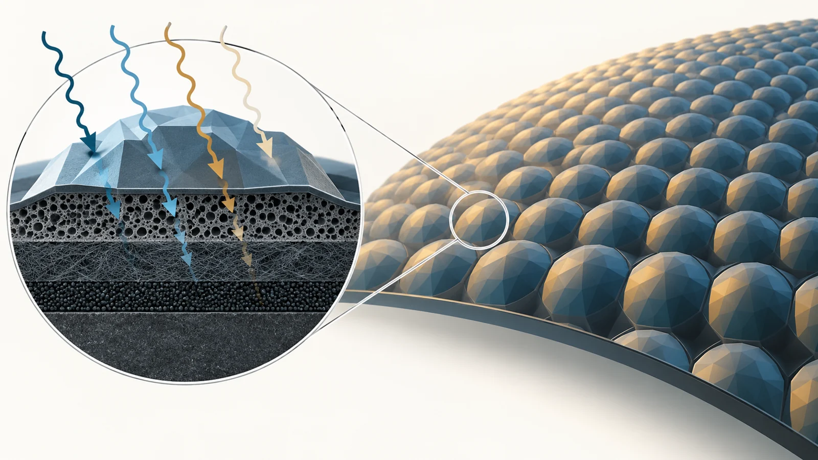
A study published on April 25, 2025, approaches that challenge at two scales. The researchers first made a layered absorbing material and reported its reflection-loss performance. They also report fabricating an absorber device using the material and separately evaluating a larger compound-eye-inspired structure in simulation. The material results and the wider device result are different kinds of evidence, and keeping them separate is key to understanding the claim.
Layers designed to help waves enter and dissipate
The material, named FCIP@SiO2@Ppy, combines functional layers with interfaces between them. In plain terms, the design aims to avoid simply turning an incoming wave away at the surface: waves that enter the material can be dissipated within it. The authors attribute the material’s performance to the way its heterogeneous interfaces form a magnetoelectric coupling network and help match the material’s impedance to that of incoming electromagnetic waves.
Impedance matching describes how well a boundary lets energy pass into a material rather than reflecting it. The study’s explanation is that the combined layers and interfaces help create that match while supporting absorption. This is the authors’ account of the design; the abstract does not provide enough detail to assess the contribution of each layer separately.
A sharp result at one frequency, and a wider material window
For the synthesized material, the researchers report a reflection loss of −66.66 dB at 9.95 GHz. Reflection loss describes energy returned from the material; a more negative value indicates less reflected energy at that frequency. The number is a peak result at one frequency, not a description of performance across the full microwave range.
They also report a 5.92 GHz absorption bandwidth using a threshold of reflection loss at or below −10 dB. That bandwidth is the span over which the material meets the stated threshold. It gives a broader picture than the single-frequency peak, but it still belongs to the material result. The two figures answer different questions: how low reflection became at one point, and how wide a frequency interval met a defined criterion.
The device’s wider range comes from simulation
The authors report fabricating an absorber device using the material. For the larger-scale design, inspired by the many small visual units of an arthropod compound eye, they report a simulated absorption range from 2.75 to 18 GHz at a thickness of 12 mm. The structure adds a macroscopic design to the material’s microscopic layered structure, with the goal of extending absorption across frequencies.
The abstract presents that 2.75–18 GHz range as a simulation result. It does not establish that a fabricated device physically reproduced the full range at 12 mm thickness, nor does it give test conditions for such a physical confirmation. A fabricated device is reported, but its existence alone does not convert the simulated range into a measured device result.
For readers, the open comparison is specific: would a physical device show the simulated wide frequency range when tested, and under what conditions? Until that is established, the reported material bandwidth and simulated device range should not be treated as interchangeable. The abstract also does not establish performance in an installed system or under particular operating conditions.
What broader microwave absorption could make practical
If physical devices reproduce the simulated range at a useful thickness and under relevant operating conditions, engineers could design compact absorbing surfaces for equipment that needs to control reflections across several microwave bands. The potential benefit would come from pairing a material with a broad response and a larger structure that extends useful absorption across frequencies. The study offers a design direction; whether it translates into that practical capability depends on the device performance holding up outside simulation.
Key Sources
- Primary source: From Magnetoelectric Core-Shell Structure to Compound Eye-Inspired Metamaterials: Multiscale Design of Ultra-Wideband Electromagnetic Wave Absorber Device.
DOI or Journal Page · Peer-Reviewed Paper · 2025-04-25
Keep exploring